Surface Activated Bonding (SAB) is a unique bonding method in which material surfaces are cleaned and activated in vacuum and then simply brought into contact at room temperature to form a strong bond. It can be applied not only to metals but also to a wide variety of materials, including semiconductors, ceramics and plastics. In recent years, bonding in ambient air has also become possible.
Room-temperature bonding is no longer a dream
Room-temperature bonding as a practical, mass-production technology
· Depending on the conditions, bonding in ambient air is also possible, and room-temperature processing enables high throughput.
· Mass-production equipment is now commercially available from IMSI member equipment manufacturers.
Proposals for pioneering new processes
· In addition to semiconductors and metals, polymer films and glass can now be bonded, and hybrid bonding of these materials with metals and semiconductors has become possible.
· We are also developing high-temperature reversible interconnects that are formed at room temperature, withstand high-temperature processing and can be debonded at room temperature.
Expanding fields of application
· In semiconductors and microelectronics, practical use and mass production have begun in low-temperature bonding for 3D integration, component manufacturing by bonding piezoelectric single-crystal substrates, and MEMS packaging.
· Applications are also advancing in multi-junction solar cells, Si photonics devices, power modules and the encapsulation of organic EL displays.
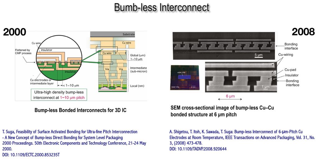 Bumpless interconnect (2000 and 2008) Bumpless interconnect (2000 and 2008)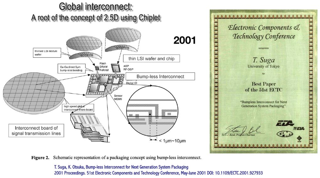 Global interconnect: the origin of the 2.5D packaging concept using chiplets (2001) Global interconnect: the origin of the 2.5D packaging concept using chiplets (2001)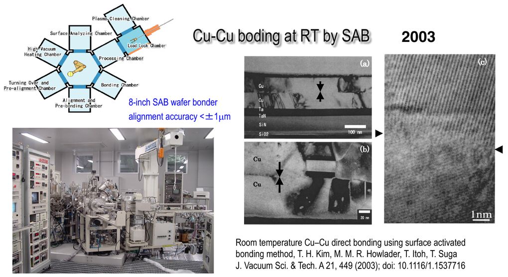 Room-temperature Cu-Cu direct bonding by Surface Activated Bonding (SAB) (2003) Room-temperature Cu-Cu direct bonding by Surface Activated Bonding (SAB) (2003)Extensions of surface activated bonding
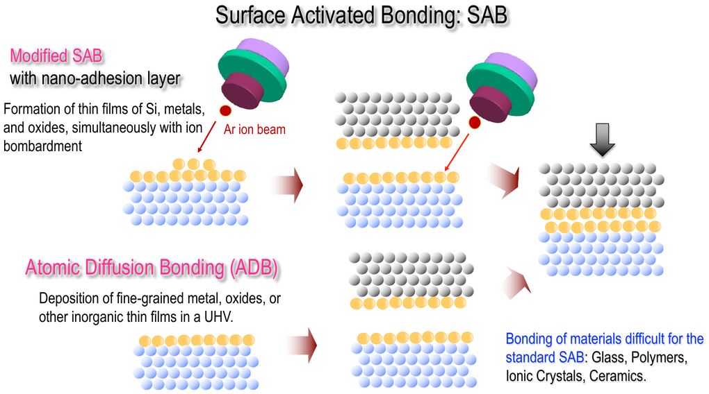
Atomic Diffusion Bonding (ADB)
· In ultra-high vacuum, ultra-thin metal or inorganic films a few nanometers thick are sputter-deposited onto the surfaces of the two substrates, which are then brought into contact without breaking the vacuum. Atomic diffusion at the film interface and grain boundaries produces a strong bond at room temperature.
· Bonding is possible with a variety of metal films such as Ti, Au and Pt, as well as oxide and nitride films, regardless of the substrate material and uniformly over the entire wafer.
· By making the films extremely thin, transparent bonds with almost no optical absorption can be obtained, and applications are advancing in optical devices, piezoelectric devices and wafer-level sealing of MEMS.
· IMSI regards ADB as a leading room-temperature bonding method alongside SAB and pursues research on both as complementary technologies.
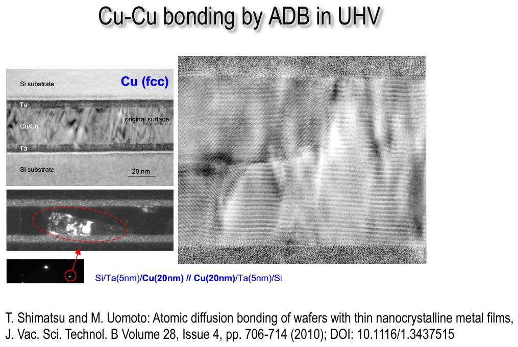 Cu-Cu bonding by Atomic Diffusion Bonding (ADB) in ultra-high vacuum Cu-Cu bonding by Atomic Diffusion Bonding (ADB) in ultra-high vacuumModified SAB
· Beyond oxide removal by ion bombardment, low-temperature bonding under atmospheric pressure (below 200 °C) has become possible using formic acid activation with a platinum catalyst.
· Combining the exposure of dangling bonds by ion bombardment with hydrophilization has enabled low-temperature bonding in ambient air (below 200 °C).
· By introducing intermediate layers of Au or Si (nano-adhesion layers), room-temperature bonding has been extended to glass and polymer films.
What is cryogenic bonding?
· Conventionally, bonding below 200 °C, that is, above room temperature but below soldering temperatures or the temperatures at which thermal diffusion bonding of Cu becomes difficult, has been called "low-temperature bonding". Recently, however, it has been found that surface activation enables direct bonding even below room temperature, at liquid-nitrogen temperature. This shows that literally "cryogenic bonding" is possible, and elucidation of its mechanism is anticipated.
|