Home | Home Japanese | Sessions and Keynotes | Author's Info | Download
Program | Social Event | Hotel | Location | Registration
Committee | Sponsors | Contact
Program | Social Event | Hotel | Location | Registration
Committee | Sponsors | Contact
|
|
Home | Home Japanese | Sessions and Keynotes | Author's Info | Download
Program | Social Event | Hotel | Location | Registration Committee | Sponsors | Contact |
|
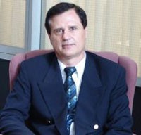
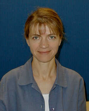
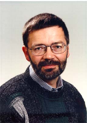
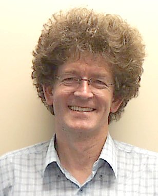
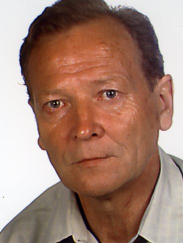
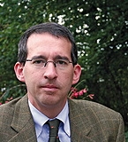
Helmut BAUMGART: Strain Engineered Silicon-on-Insulator (sSOI) Technology by Wafer Bonding and Layer Transfer (abstract) Professor, Old Dominion University Dr. Baumgart is professor of Electrical and Computer Engineering at Old Dominion University in Norfolk, Virginia, where he holds the VMEC Endowed Chair. He received his Ph.D. degree in physics from the University of Stuttgart, Germany (1981)), while performing his Ph.D. research at the Max-Planck Institute of Solid State Research in Stuttgart. Before joining Old Dominion University he has pursued a long career in the high tech industry, where he held numerous R&D positions in the microelectronics industry. He has worked extensively in SOI research at AT&T Bell Laboratories; at Royal Philips Electronics' Briarcliff Research Laboratories and at their Natuurkundig Laboratorium in Eindhoven; at IBM Microelectronics at the Advanced Semiconductor Technology Center (ASTC); at Infineon Technologies in Richmond, and at Motorola's Advanced Products Research & Development Laboratories (APRDL) in Austin. In his research areas he has authored and co-authored over 60 papers, he has published and edited 8 Electrochemical Society Conference Proceedings Volumes; he has delivered 27 conference presentations including numerous invited talks, and holds three U.S. Patents and 15 Patent Disclosures and is the recipient of numerous industry awards. Dorota TEMPLE: Overview of 3-D Integration Technology (abstract) Associate Director, Center for Materials and Electronic Technologies, RTI Dr. Dorota Temple is an Associate Director in the Center of Materials and Electronics Technologies of RTI International. She received her Ph.D. degree in solid-state physics from the AGH University of Science and Technology in Cracow, Poland. Dr. Temple has over 15 years of experience in the development of electronic materials and processes for integrated circuits, displays and sensors. Her recent interests include 3-D integration technologies for highly integrated microsystems. She has authored over 100 publications, including several invited review papers, and holds 6 U.S. patents. Mattias PETZOLD: Mechanical Reliability of Wafer-Bonded Microsystem (abstract) Professor, Fraunhofer Institute for Mechanics of Materials Matthias Petzold received his PhD degree in Physics from the Martin-Luther-University Halle-Wittenberg, Germany, in 1986. After working at the university and for a ceramics company, he changed to the Fraunhofer-Institute for Mechanics of Materials Halle, Germany, in 1992. In 1999 he became the head of the Microstructure and Diagnostics research group of the institute’s Micro- and Nanotechnology department in Halle, and the deputy head of the institute’s branchlab in Halle in 2002. The German Fraunhofer-Gesellschaft undertakes applied research of direct utility to private and public enterprises and of wide benefit to society. In this context, the primary research activities of Matthias Petzolds group are primarily focused on industrial research of recent microelectronics components and microsystems, but cover also the microstructure analysis of biomaterials, such as dental materials. Since 2007, he works additionally as a honorary professor at the University of Applied Science in Merseburg, Germany.
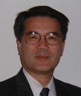
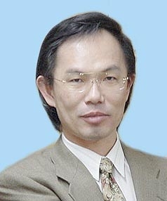
Hubert MORICEAU : Low temperature direct bonding processes: attractive ways for 3D device integrations (abstract) Doctor, CEA Léti Hubert Moriceau graduated from Ecole Nationale Supérieure de Physique de Grenoble in 1977. In 1981, he received a PhD in Materials Science. Since joining CEA-LETI in 1978, he had focused on material elaboration process for various application fields, such as magnetics, high Tc superconductors and semiconductor devices. Since 1995, he has been mainly involved in film and device transfers. He has focused on the SmartCut™ technology and more generally is in charge of some direct bonding processes to carry out BSOI structures, bonded SOI-type structures, thin film and device transfers, bonded heterostructures, 3D device integrations... and is involved in material reliability issues. Manfred REICHE: Low-Temperature Bonding Processes (abstract) Doctor, Max-Planck Institut für Mikrostrukturphysik,Halle Manfred Reiche is working as a scientific staff member at the Max Planck Institute of Microstructure Physics in Halle. His fields of activity include semiconductor wafer bonding and applications to microsystems technology, optical data communication, and the formation and characterization of advanced substrates (SOI, SSOI, GOI). He received his degree in crystallography from the Humboldt University of Berlin in 1974 and his PhD degree from the University of Leipzig in 1987. Piet DE MOOR: 3D Integration Technology Developments at IMEC (abstract) Doctor, IMEC Piet De Moor obtained his PhD degree in Physics from Leuven University Makoto YOSHIMI: Development of SOI Device Technology and Wafer Bonding by Smart Cut (abstract) Chief Scientist, Soitec Asia, Inc., Makoto Yoshimi received the B.S., M.S. and Ph.D. degrees in physical engineering from the University of Tokyo, Tokyo, Japan, in 1975, 1977, and 1991, respectively. In 1977, he joined the Research and Development Center, Toshiba Corporation, Kawasaki, Japan, where he was engaged in the development of SOI technology, including three-dimensional (3D) integration, recrystallization of poly-Si film using electron-beam annealing, characterization of fully-depleted SOI MOSFETs, analysis of the floating-body effect, lateral bipolar SOI transistor, low-voltage operation SOI-ALU, evaluation of SOI wafers, and so on. He served on many technical committees in the international conferences, including the IEEE International SOI Conference (1994-1997), International Conference on Solid State Devices and Materials (SSDM) (1994-1998), ITRS (International Technology Roadmap of Semiconductors) committee (1998-), and so on. In 2004, he joined Soitec Asia, Inc., where he is currently serving as VP and Chief Scientist. He has published more than 70 technical papers and filed more than 100 patents. Tadatomo SUGA : RoomCurrent Status of R&D for Low Temperature Bonding in Japan (abstract)
Professor, The University of Tokyo, Member of Japan Council of Science Tadatomo Suga received Ph.D. from University of Stuttgart in 1983, while performing his Ph.D. research at the Max-Planck Institute für Metallforschung, Stuttgart. In 1984 he became a member of Faculty of Engineering, the University of Tokyo, and since 1993, he has been professor of the School of Engineering. He is also a director of National Institute of Materials Science (NIMS) conducting Interconnect Design Group and the chair of IEEE CPMT Society Japan Chapter. His researches focus on micro-systems integration and packaging, and development of interconnect technology, especially the room temperature bonding technique for 3D integration. He has advocated also the importance of environmental aspects of packaging technology and is well known as the key organizer of Japanese roadmap of lead-free soldering and International Eco-design Conference.
|

 |
 |
 |
 |
 |
 |